產品中心
Kibra 480 Analyzer
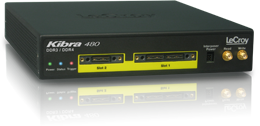
The Kibra 480 is a stand-alone protocol analyzer that provides comprehensive verification of JEDEC bus and timing issues for DDR3 and DDR4
產品文檔下載 The Teledyne LeCroy Kibra 480 is a stand-alone protocol analyzer that provides comprehensive DDR3 and DDR4 JEDEC timing analysis. Based on the ground breaking Kibra 380, the 480 platform features proprietary probing technology designed to non-intrusively monitor higher speed DDR3 as well as the new DDR4 signaling. Sitting in-line on a live system, the analyzer records memory I/O while automatically identifying timing and protocol violations. It displays both commands and errors using a full function waveform viewer allowing fast debug of memory devices and controllers.
Teledyne LeCroy developed a custom ASIC for the Kibra 480 probe to support higher speed DDR memory. This proprietary probe implementation allows loss-less capture of DDR3 to 2133 MT/s; and DDR4 to 2400 MT/s. The probes are self-powered to allow instant signal lock – including reliable capture of the DDR4 power-on sequence. Separate probes are available for DDR3 and DDR4 supporting both U-DIMM/R-DIMM as well as SO-DIMM form-factors.
Fast and Easy Debug for DDR3 and DDR4 Self-contained system offers easy connection and setup
Custom probe design supports next generation higher speed memory
No calbration needed!
Free trace viewer runs on any PC
Comprehensive JEDEC Trigger and Capture Detects over 65 JEDEC bus event & timing violations in real time
Extended recording time captures 4X the memory events vs. typical Logic Analyzer State listing
Interposers will snoop the serial presence detect (SPD) data for fast configuration of the analyzer
Dedicated trigger output to scope for Read/ Write operations
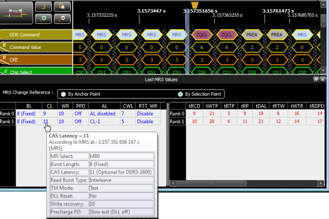
Innovative Displays Focused on Timing Analysis Traditional State and Timing Waveform views
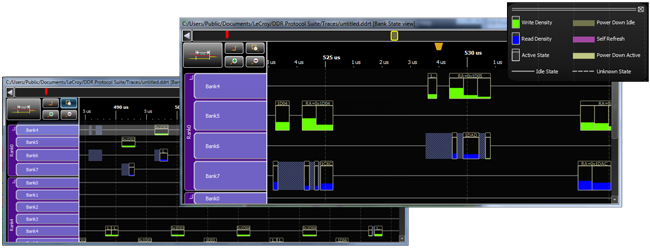
Visualize I/O distribution with the Bank State View
Bus metrics are tracked per bank and per DIMM slot
RTS view displays Bus Utilization in Real Time
Use "Row Hammer" reports to find excessive row ACTIVE commands
Flexible, Scalable Platform
Monitor two slots of quad rank DDR3 or DDR4 DIMMS concurrently
Supports registered buffered and unbuffered DIMM types
Address multi-channel application by cascading analyzers
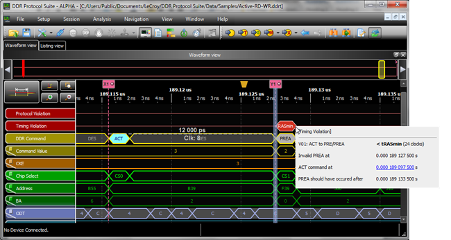
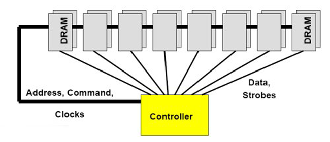
Designed specifically to overcome the cost and complexity of monolithic test approaches that rely on logic analyzer platforms, the Kibra 480 is a fully self-contained solution offering easy connection to the system under test. Using "slot interposer" style probing, the analyzer transparently monitors the link to identify over 65 JEDEC state and timing violations in real time. The tester captures address, command and control signals (ADD/CMD/CNTRL). By focusing on state-based capture and excluding the data signals, the Kibra 480 allows quick analysis of memory transactions without the time consuming calibration and setup.
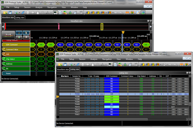
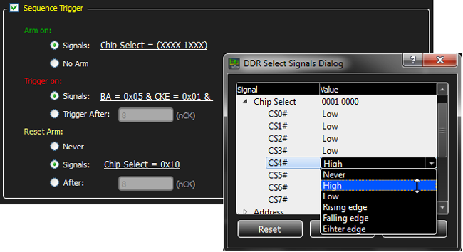
The Kibra 480 can specify custom triggers for any DDR command including MRS or Read/Write commands to a specific physical address. With the sequential triggering, the analyzer can wait for any command/control events in sequence including any combination of high/low signaling. Optionally add a timer within a sequence to specify a timeout condition or re-arm the analyzer. Filtering of NOP & Deselect commands is available to selectively capture the most important operations.
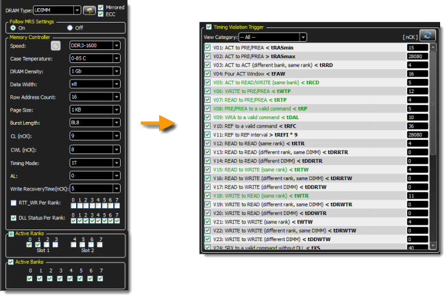
Start using the Teledyne LeCroy Kibra 480 immediately without time consuming calibration. Simply enter the memory controller parameters and start recording. The software will automatically load JEDEC timing values for the DIMM type specified. Selectively enable, disable, or customize any of the JEDEC trigger values on-the-fly. When the analyzer detects a violation, markers are placed at each error event within the Timing view to make it easy to see and verify the JEDEC timing intervals.
The latest enhancements for the Kibra 480 include the ability to Follow MRS commands on-the-fly. Enabling this option allows the Kibra system to adjust the JEDEC timing intervals in real time. In the event the memory controller sends MRS commands that change specific parameters, this prevents the Kibra from detecting false errors (ie: MRS commands that change the burst length).
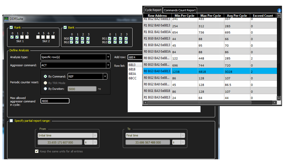
The new Row Usage report allows users to track the number of ACTIVATE commands sent to each row within a refresh cycle. Specifically designed to identify “Row Hammer” problems, it runs as a post-process to scan the trace and show any rows where excessive ACTIVATES may effect data integrity in the array. The new System Memory Map allows users to automatically translate the DRAM physical address into the logical System memory location. This allows improved correlation between processor, memory and expansion busses, such as PCI Express.
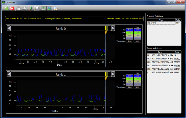
The Real Time Statistics (RTS) display tracks bus utilization and timing violations over extended periods. The RTS view shows each rank as a separate graph and can be paused, scrolled or saved to .CSV format.
Flexibility remains a hallmark of Teledyne LeCroy’s bus analyzer solutions. As an added convenience, the Kibra 480 can capture the serial presence detect (SPD) data from the bus allowing users to automatically discover and configure the memory parameters used by the system-under-test. Free downloadable software is available for sharing trace files within a development team. With its unprecedented ease of use and support for testing both DDR3 and DDR4, the Kibra 480 system allows SoC designers to leverage their R&D budgets and increase their test coverage of next generation DDR memory technology.
DDR is the acronym for Double Data-Rate Synchronous DRAM (SDRAM) and is the terminology used to describe memory used on modern computer systems. It is the successor of PC100/133 SDRAM which was primarily used prior to 1999. DDR was first introduced in 2000 and the primary advantage was its ability to fetch data on both the rising and falling edge of a clock cycle, doubling the data rate for a given clock frequency. For example, in a DDR200 device the data transfer frequency is 200 MHz, but the bus speed is 100 MHz. The DDR memory bus runs at the clock rate of 100 MHz for PC1600, 133 MHz for PC2100, 166 MHz for PC2700 and 200MHz for PC3200. However, each DDR memory module and memory chip run at an effective (data) rate of 200 MHz, 266 MHz, 333 MHz and 400MHz respectively. The computer industry has adopted a practical convention of just referring to the data rate as the DDR DIMM speed. So, PC1600 DIMMs are said to run at 200 MHz, PC2100 DIMMs at 266 MHz and so on.
Like all PC technologies, memory performance and density continue to evolve to meet the demands of faster CPUs. DDR2 was designed to deliver higher overall throughput, the main difference between DDR and DDR2 DRAM is that for DDR2 the memory cells are clocked at 1 quarter the rate of the bus. DDR2 RAM's bus frequency is boosted by electrical interface improvements, on-die termination, pre-fetch buffers and off-chip drivers. DDR2 RAM memory also uses a new form factor, a 240 pin DIMM (Dual Inline Memory Module) that is not compatible with the DDR1 standard.
| DDR2 | DDR3 | |
| Rated Speed | 400-800 Mbps | 800-1600 Mbps |
| Vdd/Vddq | 1.8V +/- 0.1V | 1.5V +/- 0.075V |
| Internal Banks | 4 | 8 |
| Termination | Limited | All DQ signals |
| Topology | Conventional T | Fly-by |
| Driver Control | OCD Calibration | Self Calibration with ZQ |
| Thermal Sensor | No | Yes (Optional) |
The newest DDR memory interface technology, DDR3, offers significant advantages over previous DDR generations. DDR3 supports data rates up to 1600 Mbps per pin with an operating voltage of 1.5 volts, a 17% reduction from the previous generation of DDR2, which operates at 1.8 volts. DDR3's built-in power conservation features, like partial refresh are desirable for mobile applications where battery power will no longer be needed just to refresh a portion of the DRAM not in active use. DDR3 also has a specification for an optional thermal sensor that allow mobile engineers to save further power by providing minimum refresh cycles.
Since DDR3 is designed to run at higher memory speeds the signal integrity of the memory module is now more important. DDR3 uses "fly-by" routing instead of the "T branches" seen on DDR2 modules. This means the address and control lines are a single path chaining from one DRAM to another, where DDR2 uses a T topology that branches on DDR2 modules. "Fly-by" takes away the mechanical line balancing and uses automatic signal time delay generated by the controller fixed at the memory system training. Each DDR3 DRAM chip has an automatic leveling circuit for calibration and to memorize the calibration data. DDR3 also uses more internal banks - 8 instead of the 4 used by DDR2 - to further speed up the system. More internal banks allow advance prefetch to reduce access latency.
All DDR memory access are burst oriented where an access starts at a selected location and continues for the burst amount. As an added complexity, Intel memory design uses interleaved burst type; with most other controllers using sequential burst type. The ability to distinguish between interleaved and sequential bursts during testing is a critical distinction when triggering on timing violations. Other complexities introduced with DDR3 include signal integrity testing on the Data lines. Because DQ/DQS are bidirectional, developers must use the DQ/DQS relationships to distinguish between Read / Write operations on the bus. Teledyne LeCroy's Kibra analyzer helps address this test challenge using dedicated, low latency SMA trigger-out to a scope for Read and Write operations (WE).
Demand from real time system developers will continue to push the evolution of memory to meet the need for improved performance, density and power efficiency.
| Host Requirements | Intel? Pentium? 4 or AMD Duron processor or greater; USB 2.0 port: 1 GB RAM (4 GB recommended; Windows? 7, Windows XP, or Windows Vista |
| Protocols Supported | DDR3 and DDR4 |
| Recording Memory Size | 4 GB |
| Data Rates Supported | DDR3 - 300 MHz – 1066 MHz DIMM clock speeds DDR4 - 800 MHz – 1200 MHz DIMM clock speeds |
| Probe Interface | DDR3: UDIMM, RDIMM, LRDIMM, SO-DIMM, SO-DIMM with ECC, SO-DIMM Non-ECC, DDR4: UDIMM, RDIMM, LRDIMM (284 & 288-pin available), SO-DIMM |
| Front Panel LEDs | Power, Status, Trigger |
| Front Panel Connectors | Cable Interface to DIMM Slot 1 Interposer, Cable Interface to DIMM Slot 2 Interposer, External RefClk-IN SMA, External Read / Write Trigger Output (SMA), Interposer Probe Power Connector |
| Rear Panel Connectors | CrossSync Connector, USB 2.0 Connection to Host PC: Trigger IN SMA, Trigger OUT SMA |
| Dimensions | (W x H x D) 20 x 3.2 x 23 cm (8”W x 1.25”H x 9”D) |
| Weight | 1.5 Kg (3.4 lbs) |
| Power Requirements | External 12V power |
| Environmental | Operating 0 to 55 °C (32 to 131 °F), Non-operating -20 to 80 °C (-4 to 176) Humidity: 10 to 90% RH (non-condensing) |
 021-64867827?/ 64865993
 shanghai@leco-tech.com