產(chǎn)品中心
Kibra 480 Compliance System
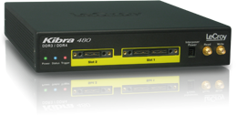
The Kibra 480 Compliance System allows DDR memory developers, implementers and integrators a cost effective solution to verify and validate that their DDR memory solution meets JEDEC compliance parameters
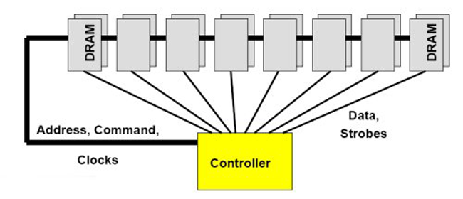
產(chǎn)品文檔下載The Kibra 480 Compliance Analyzer provides DDR memory developers, implementers and integrators a cost effective solution to verify and validate that their DDR memory solution meets JEDEC compliance parameters. Kibra 480 supports either DDR3 or DDR4. The quick and easy hardware setup and immediate feedback on violations allow users to quickly validate their memory system meets JEDEC timing compliance or swiftly identify problem areas with their memory system. Capturing the Command Address and Control bus, the Kibra 480 can quickly identify timing issues associated with the JEDEC defined speed bins.
Simply Program the memory settings for your hardware system and initiate recordings. There is no calibration requirement, as the Kibra 480 uses a unique probing implementation to handle setup and hold times. This allows for quick setup and testing of memory system compliance.
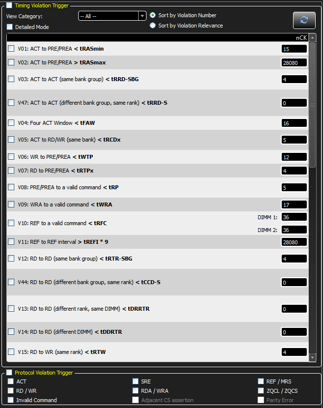
After setup, the Kibra 480 DDR3/DDR4 compliance analyzer will begin recording and trigger on any of 60 plus JEDEC violations. On upload a concise report of all violations recorded will be opened. Violations can be examined to determine the cause and timing of the violations.
The Kibra 480 comes with 4Gigabytes of recording memory and will only trigger on any defined violation. This allows for long recording capability. JEDEC violations can be loaded based on the defined speed bin of the system under test, or modified by users for custom timing parameters. Over 50 Timing and protocol violations are continuously monitored The across 2DIMMs Per Channel, Four (4) Ranks per DIMM and 8 Banks per rank for DDR3 or 4 Bank Groups per Rank and 4 Banks per Bank Group. This allows for compliance monitoring of over 3200 violations across up to 64 banks of memory simultaneously.
On determination of any JEDEC violations, the Kibra 480 Compliance Analyzer will upload a detailed report of all violations, along with a summary report. Violations are detailed and referenced to the JEDEC parameter. The easy to read report can also be exported to CSV for easy manipulation.
Designed to support a multitude of DIMM options, the Kibra 480 Compliance Analyzer can be used with UDIMM, RDIMM, LRDIMM as well as all flavors of SODIMM, including DDR3 SOUDIMM with ECC and DDR3 SORDIMM
DDR is the acronym for Double Data-Rate Synchronous DRAM (SDRAM) and is the terminology used to describe memory used on modern computer systems. It is the successor of PC100/133 SDRAM which was primarily used prior to 1999. DDR was first introduced in 2000 and the primary advantage was its ability to fetch data on both the rising and falling edge of a clock cycle, doubling the data rate for a given clock frequency. For example, in a DDR200 device the data transfer frequency is 200 MHz, but the bus speed is 100 MHz. The DDR memory bus runs at the clock rate of 100 MHz for PC1600, 133 MHz for PC2100, 166 MHz for PC2700 and 200MHz for PC3200. However, each DDR memory module and memory chip run at an effective (data) rate of 200 MHz, 266 MHz, 333 MHz and 400MHz respectively. The computer industry has adopted a practical convention of just referring to the data rate as the DDR DIMM speed. So, PC1600 DIMMs are said to run at 200 MHz, PC2100 DIMMs at 266 MHz and so on.
Like all PC technologies, memory performance and density continue to evolve to meet the demands of faster CPUs. DDR2 was designed to deliver higher overall throughput, the main difference between DDR and DDR2 DRAM is that for DDR2 the memory cells are clocked at 1 quarter the rate of the bus. DDR2 RAM's bus frequency is boosted by electrical interface improvements, on-die termination, pre-fetch buffers and off-chip drivers. DDR2 RAM memory also uses a new form factor, a 240 pin DIMM (Dual Inline Memory Module) that is not compatible with the DDR1 standard.
| DDR2 | DDR3 | |
| Rated Speed | 400-800 Mbps | 800-1600 Mbps |
| Vdd/Vddq | 1.8V +/- 0.1V | 1.5V +/- 0.075V |
| Internal Banks | 4 | 8 |
| Termination | Limited | All DQ signals |
| Topology | Conventional T | Fly-by |
| Driver Control | OCD Calibration | Self Calibration with ZQ |
| Thermal Sensor | No | Yes (Optional) |
The newest DDR memory interface technology, DDR3, offers significant advantages over previous DDR generations. DDR3 supports data rates up to 1600 Mbps per pin with an operating voltage of 1.5 volts, a 17% reduction from the previous generation of DDR2, which operates at 1.8 volts. DDR3's built-in power conservation features, like partial refresh are desirable for mobile applications where battery power will no longer be needed just to refresh a portion of the DRAM not in active use. DDR3 also has a specification for an optional thermal sensor that allow mobile engineers to save further power by providing minimum refresh cycles.
Since DDR3 is designed to run at higher memory speeds the signal integrity of the memory module is now more important. DDR3 uses "fly-by" routing instead of the "T branches" seen on DDR2 modules. This means the address and control lines are a single path chaining from one DRAM to another, where DDR2 uses a T topology that branches on DDR2 modules. "Fly-by" takes away the mechanical line balancing and uses automatic signal time delay generated by the controller fixed at the memory system training. Each DDR3 DRAM chip has an automatic leveling circuit for calibration and to memorize the calibration data. DDR3 also uses more internal banks - 8 instead of the 4 used by DDR2 - to further speed up the system. More internal banks allow advance prefetch to reduce access latency.
All DDR memory access are burst oriented where an access starts at a selected location and continues for the burst amount. As an added complexity, Intel memory design uses interleaved burst type; with most other controllers using sequential burst type. The ability to distinguish between interleaved and sequential bursts during testing is a critical distinction when triggering on timing violations. Other complexities introduced with DDR3 include signal integrity testing on the Data lines. Because DQ/DQS are bidirectional, developers must use the DQ/DQS relationships to distinguish between Read / Write operations on the bus. Teledyne LeCroy's Kibra analyzer helps address this test challenge using dedicated, low latency SMA trigger-out to a scope for Read and Write operations (WE).
Demand from real time system developers will continue to push the evolution of memory to meet the need for improved performance, density and power efficiency.
| Host Requirements | Intel? Pentium? 4 or AMD Duron processor or greater; USB 2.0 port: 1 GB RAM (4 GB recommended; Windows? 7, Windows XP, or Windows Vista |
| Protocols Supported | DDR3 and DDR4 |
| Recording Memory Size | 4 GB |
| Data Rates Supported | DDR3 - 300 MHz – 1066 MHz DIMM clock speeds DDR4 - 800 MHz – 1200 MHz DIMM clock speeds |
| Probe Interface | DDR3: UDIMM, RDIMM, LRDIMM, SO-DIMM, SO-DIMM with ECC, SO-DIMM Non-ECC, DDR4: UDIMM, RDIMM, LRDIMM (284 & 288-pin available), SO-DIMM |
| Front Panel LEDs | Power, Status, Trigger |
| Front Panel Connectors | Cable Interface to DIMM Slot 1 Interposer, Cable Interface to DIMM Slot 2 Interposer, External RefClk-IN SMA, External Read / Write Trigger Output (SMA), Interposer Probe Power Connector |
| Rear Panel Connectors | CrossSync Connector, USB 2.0 Connection to Host PC: Trigger IN SMA, Trigger OUT SMA |
| Dimensions | (W x H x D) 20 x 3.2 x 23 cm (8”W x 1.25”H x 9”D) |
| Weight | 1.5 Kg (3.4 lbs) |
| Power Requirements | External 12V power |
| Environmental | Operating 0 to 55 °C (32 to 131 °F), Non-operating -20 to 80 °C (-4 to 176) Humidity: 10 to 90% RH (non-condensing) |
 021-64867827?/ 64865993
 shanghai@leco-tech.com